pcb - What is the pad size required for this BGA AW H3 Chip? - Electrical Engineering Stack Exchange
By A Mystery Man Writer
Description
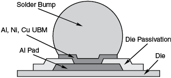
I'm trying to figure out the pad size to use for my footprint according to this datasheet.The last page in the datasheet has the package dimensions. I've also posted the relevant information in a p
![pcb - What is the pad size required for this BGA AW H3 Chip? - Electrical Engineering Stack Exchange](https://www.mouser.com/datasheet/lrg/389/stm32h573ai-3107220.jpg)
Datasheet - STM32H573xx - Arm® Cortex®-M33 32-bit MCU+TrusZone®
![pcb - What is the pad size required for this BGA AW H3 Chip? - Electrical Engineering Stack Exchange](https://ctt-pcb.com/wp-content/uploads/2021/12/HDI21.png)
What is HDI PCB? Application technology of HDI Flex PCB, PCB and PCBA production experts from China
Designing Manufacturable and Reliable Printed Circuit Boards Employing Chip-Scale eGaN FETs
![pcb - What is the pad size required for this BGA AW H3 Chip? - Electrical Engineering Stack Exchange](https://i.stack.imgur.com/gMMZw.png)
power supply - What is the PAD size required for the Battery negative and Positive pads voltage (min 30v to max 42v) current (min 500 mA to max 15 A)? - Electrical Engineering Stack Exchange
Lenovo Thinkpad X100E (Quanta FL3 Congo) PDF, PDF, Computer Networking
![pcb - What is the pad size required for this BGA AW H3 Chip? - Electrical Engineering Stack Exchange](https://cdn-0.fccid.io/img.php?id=941147&img=bg4e.png)
863P3 Quad-Band GSM/GPRS module -Model: GE863-PRO3 User Manual Manual Telit Communications S.p.A.
![pcb - What is the pad size required for this BGA AW H3 Chip? - Electrical Engineering Stack Exchange](https://www.ironwoodelectronics.com/wp-content/uploads/2021/05/C14391b_460x350.jpg)
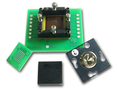
BGA Sockets - Ironwood Electronics
![pcb - What is the pad size required for this BGA AW H3 Chip? - Electrical Engineering Stack Exchange](https://www.intel.com/content/dam/docs/us/en/683132/current/joc1463009376617.png)
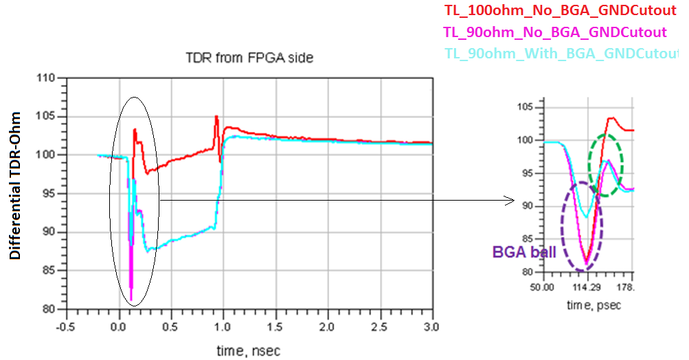
GND Cutout Under BGA Pads in Fan-out Configuration
PCB Stack Up and Component Layout for Kabini APU Motherboard, PDF, Digital Technology
What is a pad stack in PCB? - Quora
![pcb - What is the pad size required for this BGA AW H3 Chip? - Electrical Engineering Stack Exchange](https://epc-co.com/epc/Portals/0/epc/blogs/Soldermask%20defined%20%20versus%20non-soldermask%20defined.png)
Designing Manufacturable and Reliable Printed Circuit Boards Employing Chip-Scale eGaN FETs
![pcb - What is the pad size required for this BGA AW H3 Chip? - Electrical Engineering Stack Exchange](https://www.schmalztech.com/cdn/shop/files/ST-PERF-2-3_front_1024x1024@2x.jpg?v=1701523613)
2 x 3 Perfboard, Electronics Prototyping
from
per adult (price varies by group size)