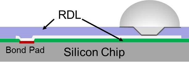
The bond pad redistribution layer (polyimide 1) and the under bump
By A Mystery Man Writer
Description

Process and Key Technology of Typical Advanced Packaging

Chip Scale Packaging Helps Portable Medical Devices Save Size and Weight

Warren FLACK, Vice President, PhD

WO2018237377A1 - Curable polyimides - Google Patents

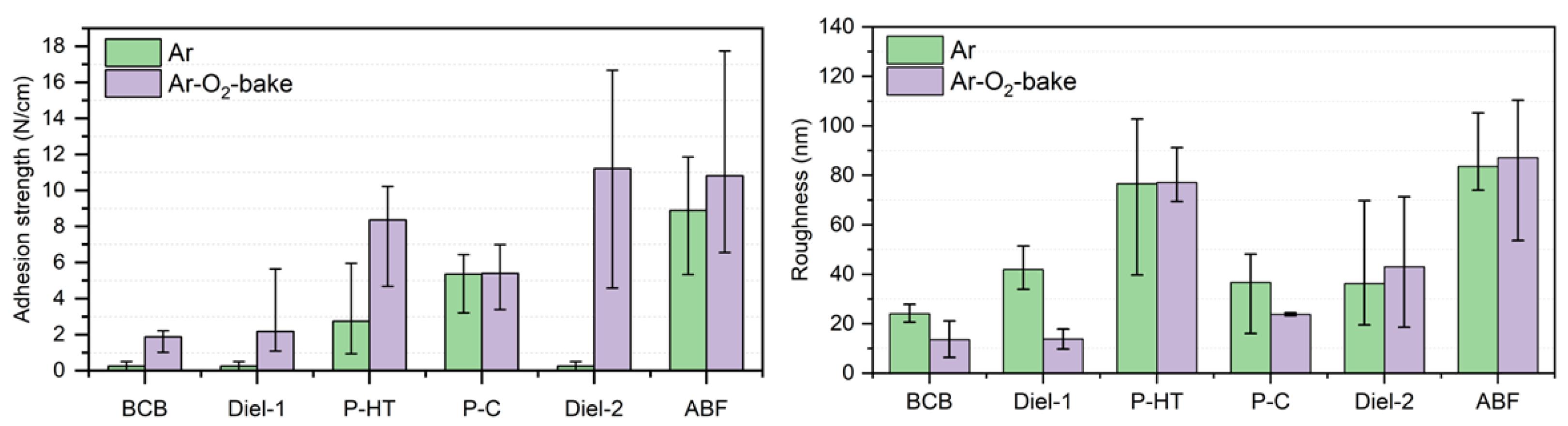
Electromigration Performance Of Fine-Line Cu Redistribution Layer (RDL) For HDFO Packaging

The bond pad redistribution layer (polyimide 1) and the under bump
Polymers, Free Full-Text

Wafer level packaging having bump-on-polymer structure - ScienceDirect

Polymers, Free Full-Text

Redistribution in wafer level chip size packaging technology for high power device applications: Process and design considerations - ScienceDirect

The bond pad redistribution layer (polyimide 1) and the under bump
Polymer Challenges in Electronic Packaging: Part 8 Embedded Wafer Level Packaging Materials - Polymer Innovation Blog

Electromigration Performance Of Fine-Line Cu Redistribution Layer (RDL) For HDFO Packaging
from
per adult (price varies by group size)