Schematic of channels with (a) non-overlapped electrical double layers
By A Mystery Man Writer
Description
Wi-Fi: Overview of the 802.11 Physical Layer and Transmitter

What is a Pad in PCB Design and Development
/documentation/sites/default/files/w
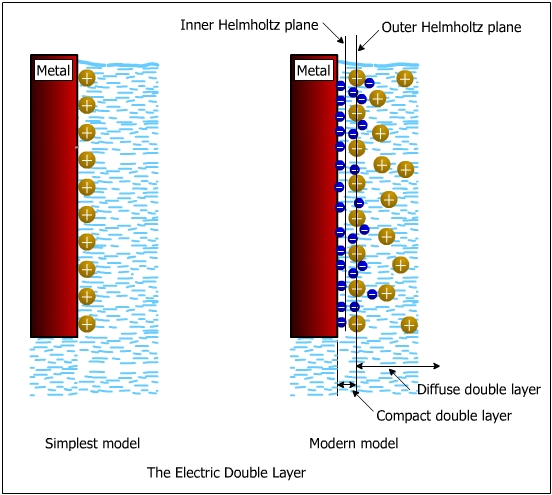
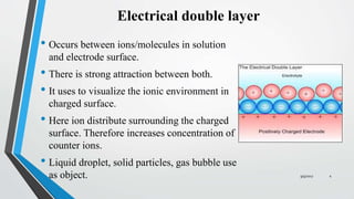
Electric Double Layer
Comparing Single-Sided PCBs vs. Double-Sided PCBs
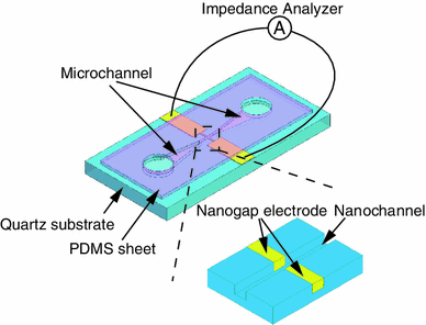
Direct measurement of electric double layer in a nanochannel by

PDF) Theory and experiments of concentration polarization and ion focusing at microchannel and nanochannel interfaces
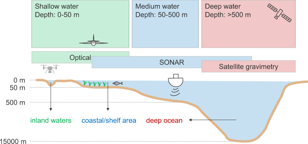
A REVIEW OF ACTIVE AND PASSIVE OPTICAL METHODS IN HYDROGRAPHY - IHR
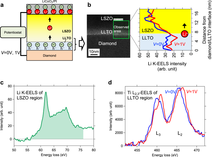
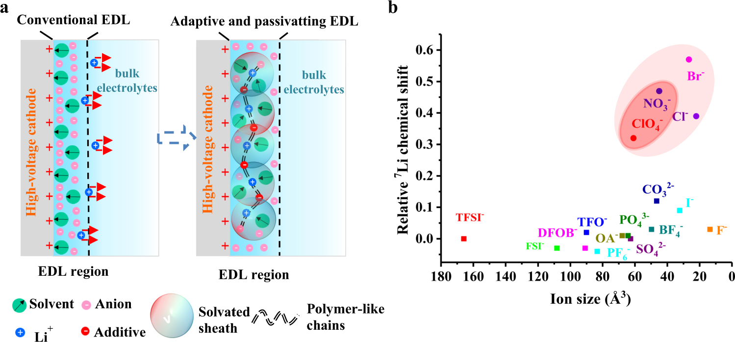
The electric double layer effect and its strong suppression at Li+

PDF) Theory and experiments of concentration polarization and ion focusing at microchannel and nanochannel interfaces

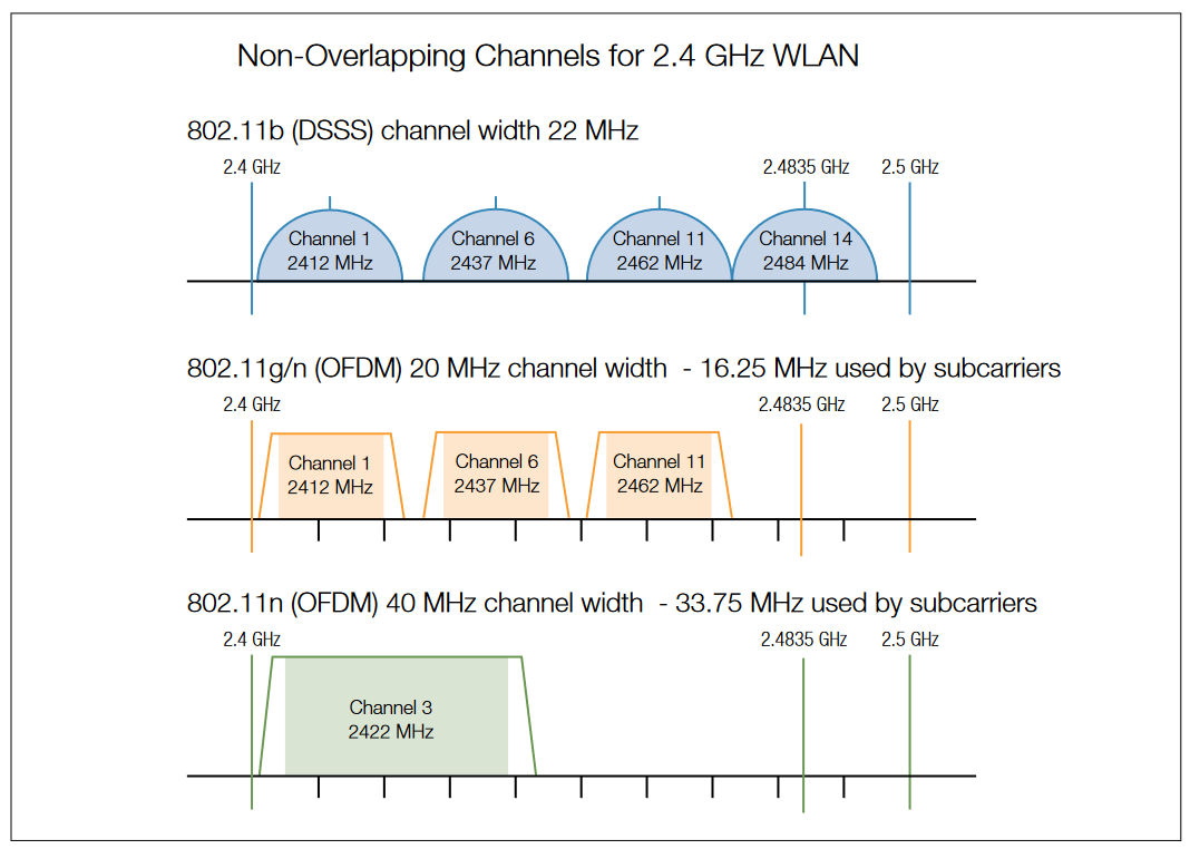
List of WLAN channels - Wikipedia

The Pros And Cons Of Having Multiple Layers Of Management - Insperity

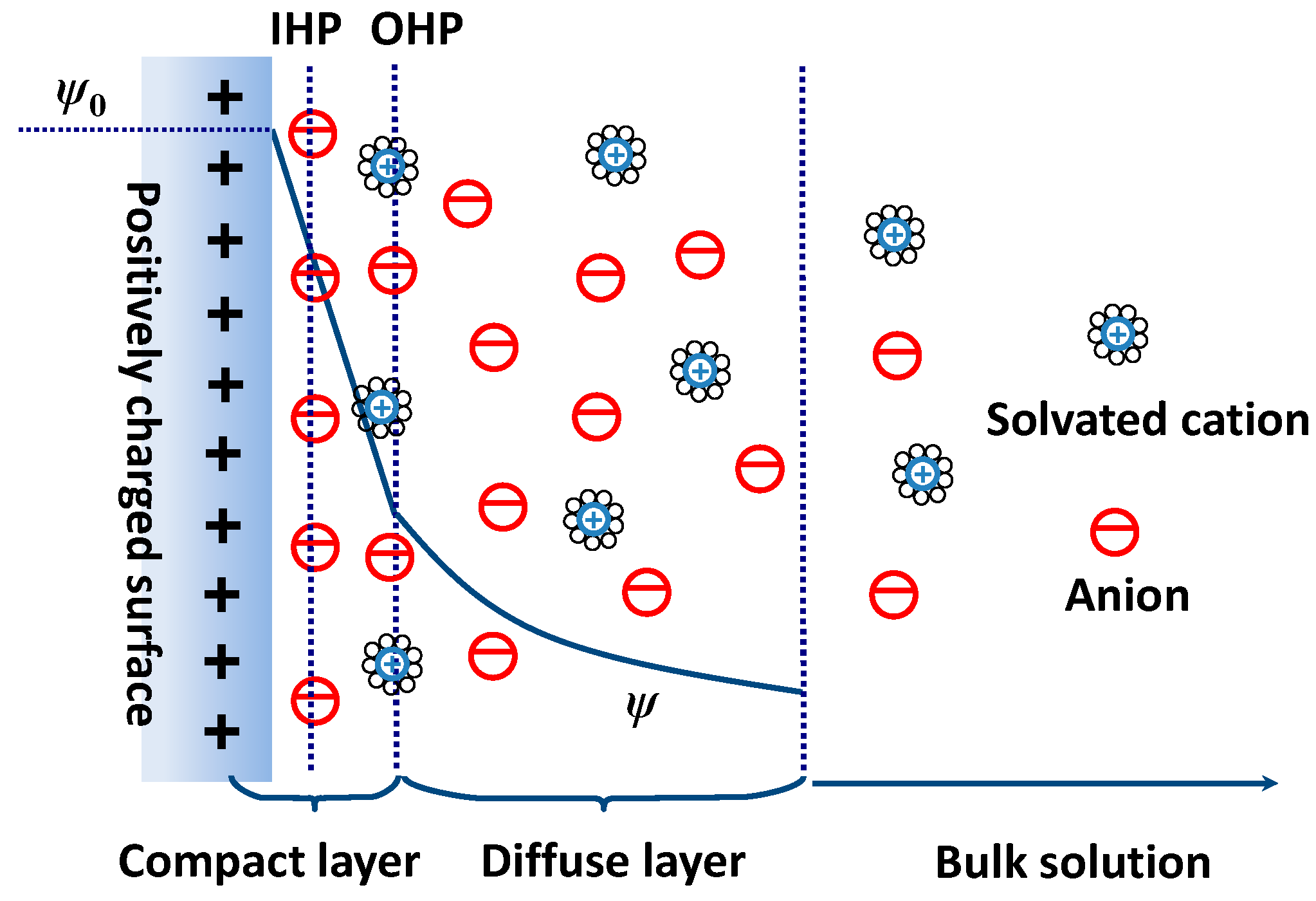
Schematic representation of electrolyte influence on electrical
from
per adult (price varies by group size)