PDF] Under Bump Metallurgy (UBM)-a technology review for flip chip packaging
By A Mystery Man Writer
Description
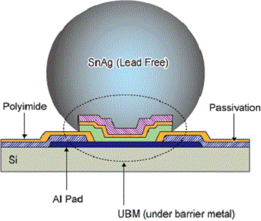
Flip chip packaging technology has been utilized more than 40 years ago and it still experiencing an explosives growth. This growth is driven by the need for high performance, high volume, better reliability, smaller size and lower cost of electronic consumer products. Wafer bumping is unavoidable process in flip chip packaging, thus, picking the correct bumping technology that is capable of bumping silicon wafer at high yield and a high reliability with lower cost is challenging. This paper discusses the available wafer bumping technologies for flip chip packaging. The discussion will be focused on process assembly, solder ball compatibility, design structure and lastly cost which translated to overall product costs.
![PDF] Under Bump Metallurgy (UBM)-a technology review for flip chip packaging](https://d3i71xaburhd42.cloudfront.net/33cac6292e50b744dfb0c90a36310462259f3624/3-Figure4-1.png)
PDF] Under Bump Metallurgy (UBM)-a technology review for flip chip packaging
Cost, production, and logistics implications of C4NP solder bumping. - Document - Gale Academic OneFile
![PDF] Under Bump Metallurgy (UBM)-a technology review for flip chip packaging](https://i1.rgstatic.net/ii/profile.image/276059736244231-1442829178858_Q64/Philip-Chan-20.jpg)
PDF) Under bump metallurgy (UBM) - A technology review for flip
![PDF] Under Bump Metallurgy (UBM)-a technology review for flip chip packaging](https://i1.rgstatic.net/publication/3424982_Pb-free_Sn35Ag_electroplating_bumping_process_and_under_bump_metallization_UBM/links/00b4953317101715dd000000/largepreview.png)
PDF) Pb-free Sn/3.5Ag electroplating bumping process and under bump metallization (UBM)
![PDF] Under Bump Metallurgy (UBM)-a technology review for flip chip packaging](https://image.isu.pub/170124101630-5d8bc5f46b229b21970a5ec534a49ea2/jpg/page_1.jpg)
Chipscale may jun 2016 interactive by tweenturbo - Issuu
![PDF] Under Bump Metallurgy (UBM)-a technology review for flip chip packaging](https://www.researchgate.net/profile/Muzamir-Isa/publication/242476081/figure/fig1/AS:298437070344192@1448164350417/Schematic-cross-section-of-evaporated-UBM-and-solder-bump-12_Q320.jpg)
PDF) Under bump metallurgy (UBM) - A technology review for flip
![PDF] Under Bump Metallurgy (UBM)-a technology review for flip chip packaging](https://c5.rgstatic.net/m/4671872220764/images/template/default/profile/profile_default_m.jpg)
PDF) Under bump metallurgy (UBM) - A technology review for flip
![PDF] Under Bump Metallurgy (UBM)-a technology review for flip chip packaging](https://ars.els-cdn.com/content/image/1-s2.0-S0026271405000302-gr1.jpg)
A study in flip-chip UBM/bump reliability with effects of SnPb solder composition - ScienceDirect
![PDF] Under Bump Metallurgy (UBM)-a technology review for flip chip packaging](https://pubs.acs.org/cms/10.1021/acsanm.3c04209/asset/images/large/an3c04209_0004.jpeg)
Sn–Bi–Ag Solder Enriched with Ta2O5 Nanoparticles for Flexible Mini-LED Microelectronic Packaging
![PDF] Under Bump Metallurgy (UBM)-a technology review for flip chip packaging](https://www.accessengineeringlibrary.com/sites/default/files/styles/cover_content_details/binary/mheaeworks/07037d1ff66d44d7/07ab07a8658bc39574a9df1f5613b832a1929d44bbdf4dfe6a66d741eb5eba7b/cover.jpg?itok=P8lk_YNc)
FLIP CHIP TECHNOLOGY McGraw-Hill Education - Access Engineering
![PDF] Under Bump Metallurgy (UBM)-a technology review for flip chip packaging](https://docplayer.net/docs-images/69/59958039/images/2-0.jpg)
UNDER BUMP METALLURGY (UBM)-A TECHNOLOGY REVIEW FOR FLIP CHIP PACKAGING - PDF Free Download
from
per adult (price varies by group size)