Verification of Charge Transfer in Metal-Insulator-Oxide Semiconductor Diodes via Defect Engineering of Insulator
By A Mystery Man Writer
Description
![Verification of Charge Transfer in Metal-Insulator-Oxide Semiconductor Diodes via Defect Engineering of Insulator](https://ars.els-cdn.com/content/image/3-s2.0-B9780323855884000039-f13-11-9780323855884.jpg)
Role of defects on the transparent conducting properties of binary metal oxide thin film electrodes - ScienceDirect
![Verification of Charge Transfer in Metal-Insulator-Oxide Semiconductor Diodes via Defect Engineering of Insulator](https://europepmc.org/articles/PMC6990641/bin/ao9b04011_0006.jpg)
Electron-Transport Characteristics through Aluminum Oxide (100) and (012) in a Metal-Insulator-Metal Junction System: Density Functional Theory-Nonequilibrium Green Function Approach. - Abstract - Europe PMC
![Verification of Charge Transfer in Metal-Insulator-Oxide Semiconductor Diodes via Defect Engineering of Insulator](https://www.mdpi.com/materials/materials-16-06161/article_deploy/html/images/materials-16-06161-g012-550.jpg)
Materials, Free Full-Text
![Verification of Charge Transfer in Metal-Insulator-Oxide Semiconductor Diodes via Defect Engineering of Insulator](https://media.springernature.com/full/springer-static/image/art%3A10.1038%2Fsrep01026/MediaObjects/41598_2013_Article_BFsrep01026_Fig1_HTML.jpg)
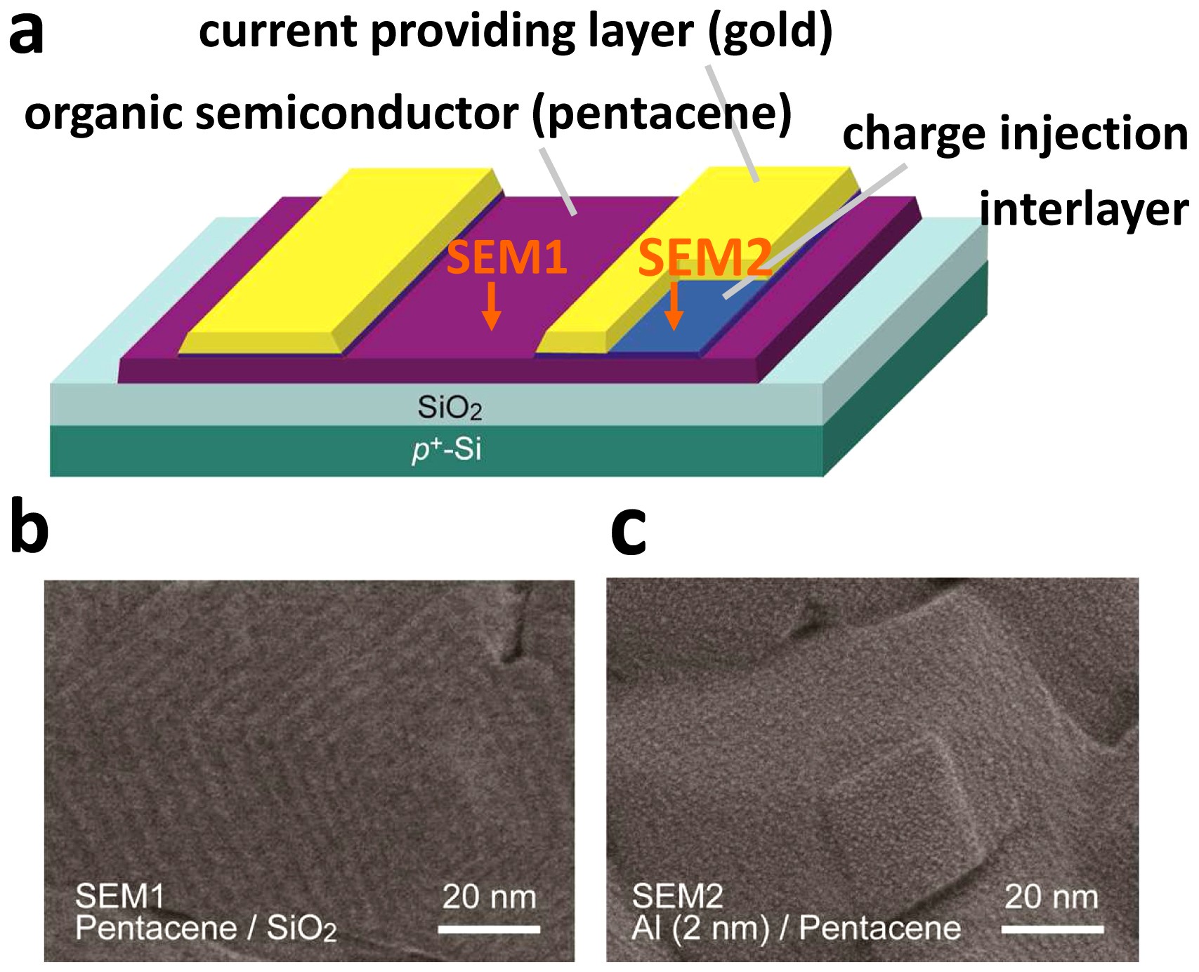
On Practical Charge Injection at the Metal/Organic Semiconductor Interface
![Verification of Charge Transfer in Metal-Insulator-Oxide Semiconductor Diodes via Defect Engineering of Insulator](https://europepmc.org/articles/PMC6990641/bin/ao9b04011_0003.jpg)
Electron-Transport Characteristics through Aluminum Oxide (100) and (012) in a Metal-Insulator-Metal Junction System: Density Functional Theory-Nonequilibrium Green Function Approach. - Abstract - Europe PMC
![Verification of Charge Transfer in Metal-Insulator-Oxide Semiconductor Diodes via Defect Engineering of Insulator](https://ars.els-cdn.com/content/image/1-s2.0-S2772949422000109-gr1.jpg)
Ion-gating analysis on conduction mechanisms in oxide semiconductors - ScienceDirect
![Verification of Charge Transfer in Metal-Insulator-Oxide Semiconductor Diodes via Defect Engineering of Insulator](https://www.researchgate.net/publication/324212292/figure/fig4/AS:611889327403008@1522897192819/Effect-of-the-electron-mobility-of-the-top-semiconductor-electrode-on-the-vertical_Q320.jpg)
Effect of the electron mobility of the top semiconductor electrode on
![Verification of Charge Transfer in Metal-Insulator-Oxide Semiconductor Diodes via Defect Engineering of Insulator](https://pubs.acs.org/cms/10.1021/acsami.8b05929/asset/images/medium/am-2018-05929v_0009.gif)
Oxygen Effect on the Properties of Epitaxial (110) La0.7Sr0.3MnO3 by Defect Engineering
![Verification of Charge Transfer in Metal-Insulator-Oxide Semiconductor Diodes via Defect Engineering of Insulator](https://d3i71xaburhd42.cloudfront.net/9f80498c678164d0c3e487f44cf12b841cd79d48/3-Figure5-1.png)
Figure 3 from Charge Trapping Memory Characteristics of Amorphous-Indium–Gallium–Zinc Oxide Thin-Film Transistors With Defect-Engineered Alumina Dielectric
![Verification of Charge Transfer in Metal-Insulator-Oxide Semiconductor Diodes via Defect Engineering of Insulator](https://ars.els-cdn.com/content/image/1-s2.0-S2772949422000109-gr3.jpg)
Ion-gating analysis on conduction mechanisms in oxide semiconductors - ScienceDirect
![Verification of Charge Transfer in Metal-Insulator-Oxide Semiconductor Diodes via Defect Engineering of Insulator](https://europepmc.org/articles/PMC7283246/bin/41598_2020_66339_Fig3_HTML.jpg)
Filamentary Resistive Switching and Capacitance-Voltage Characteristics of the a-IGZO/TiO2 Memory. - Abstract - Europe PMC
from
per adult (price varies by group size)