Electrical Double Layer based devices
By A Mystery Man Writer
Description
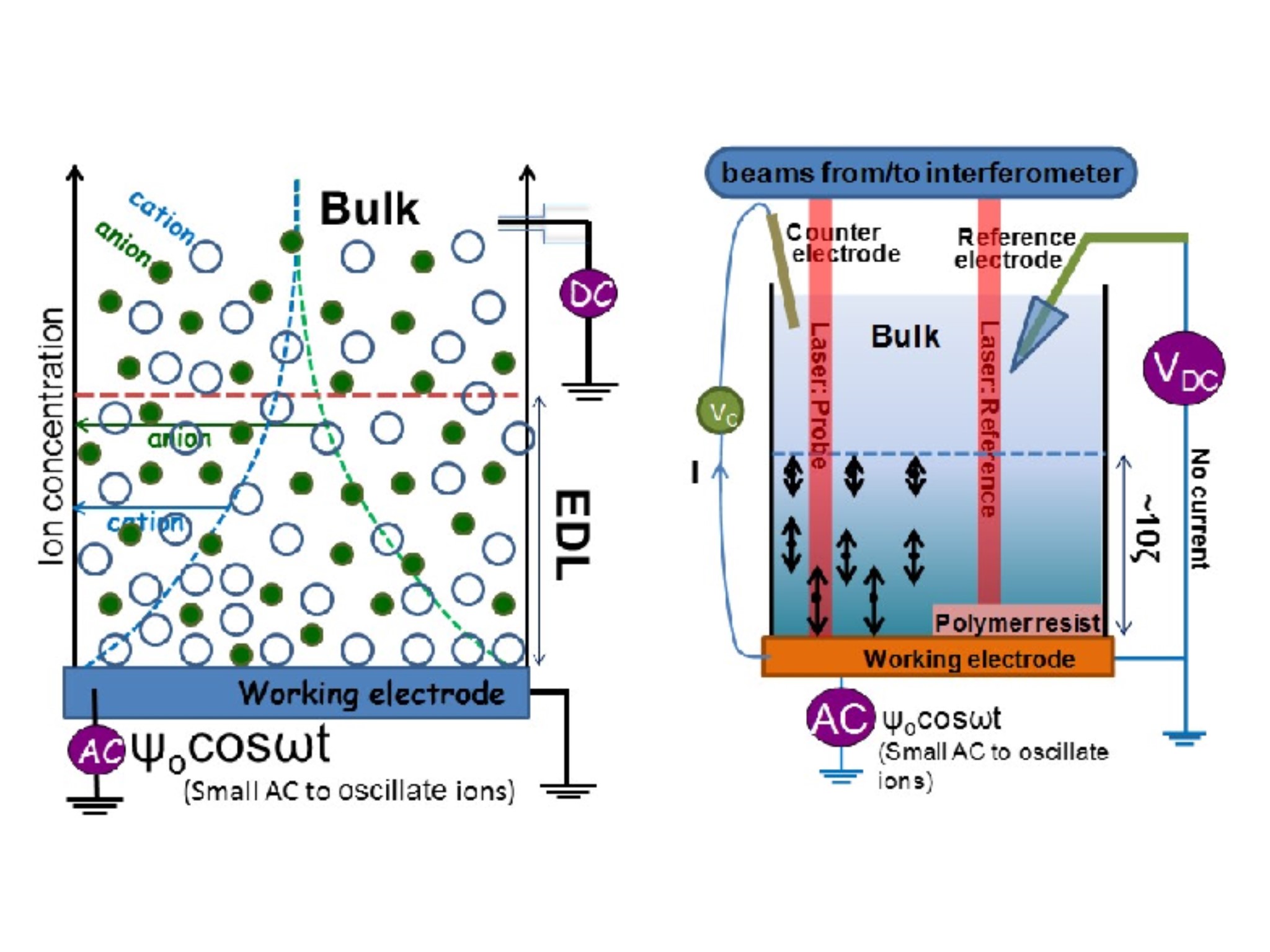
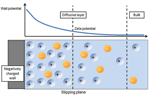
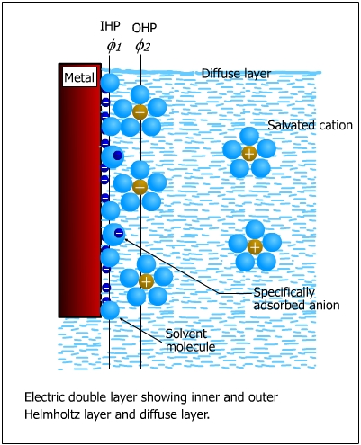
Immersing a metal (electrode) in a salt solution will spontaneously accumulate ions due to image charge to form the well known electrical double layer (EDL). Sign of the charge depends on the Fermi level (i.e., the electrochemical potential) difference between the metal and the solution. For example, gold will accumulate negative ions (i.e., anions). The interfacial structure
![Electrical Double Layer based devices](https://www.researchgate.net/publication/302584410/figure/fig2/AS:360114344218625@1462869358528/Models-of-the-electrical-double-layer-at-a-positively-charged-surface-a-the-Helmholtz.png)
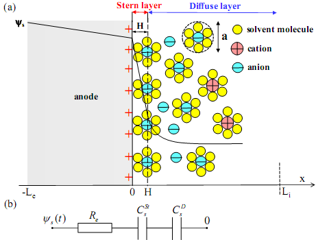
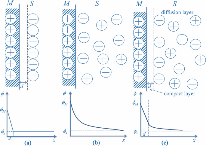
3 Models of the electrical double-layer at a positively charged
![Electrical Double Layer based devices](https://sp-uploads.s3.amazonaws.com/uploads/services/2752407/20211231191315_61cf564b558eb_nanomechanics_of_materials_and_biomaterial___lecture_14___the_electrical_double_layer__edl_page1.png)
SOLUTION: Nanomechanics of materials and biomaterial lecture 14 the electrical double layer edl - Studypool
![Electrical Double Layer based devices](https://scx1.b-cdn.net/csz/news/800a/2021/a-solid-favor-for-rese.jpg)
Electrical Double Layer Based Devices College Of, 41% OFF
![Electrical Double Layer based devices](https://www.researchgate.net/publication/281779548/figure/fig1/AS:614149973348374@1523436172623/An-example-of-the-mechanism-used-for-biomolecule-detection-Here-the-target-biomolecule_Q320.jpg)
Electrical Double Layer Based Devices College Of, 41% OFF
![Electrical Double Layer based devices](https://cdn.comsol.com/wordpress/2013/10/Electrical-double-layer.png)
Modeling Electroosmotic Flow and the Electrical Double Layer
![Electrical Double Layer based devices](https://media.springernature.com/lw685/springer-static/image/chp%3A10.1007%2F978-3-030-44995-7_10/MediaObjects/492101_1_En_10_Fig3_HTML.png)
Electrical Double-Layer Structure and Property of Ionic Liquid-Electrode System for Electrochemical Applications
![Electrical Double Layer based devices](https://d3i71xaburhd42.cloudfront.net/33da08ee1f032de6428e4fda649a19c6a49ad495/2-Figure1-1.png)
Figure 1 from Charge Regulation in the Electrical Double Layer: Ion Adsorption and Surface Interactions.
Physical Interpretations of Nyquist Plots for EDLC Electrodes and Devices
![Electrical Double Layer based devices](https://chempedia.info/pic1/087043007161035123066053061072043159057245223139.png)
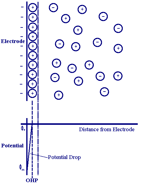
Stem-Graham model - Big Chemical Encyclopedia
![Electrical Double Layer based devices](https://www.ceb.cam.ac.uk/files/media/dlfig1.gif)
The Electrical Double Layer Department of Chemical Engineering and Biotechnology
![Electrical Double Layer based devices](https://www.matsusada.com/column/uploads/structure.png)
Electric Double-Layer Capacitors, Tech
![Electrical Double Layer based devices](https://faculty.kfupm.edu.sa/ME/hussaini/Corrosion%20Engineering/Images/doublelayer2.jpg)
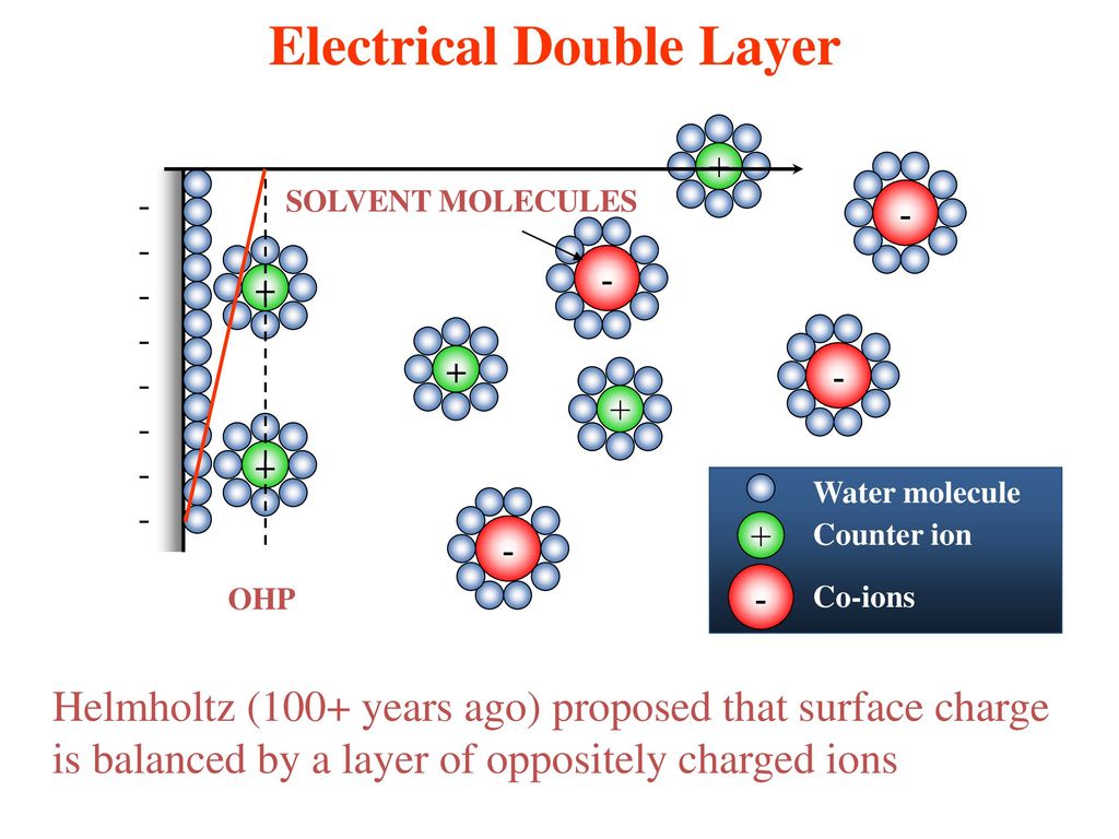
Electric Double Layer
![Electrical Double Layer based devices](https://media.springernature.com/m685/springer-static/image/art%3A10.1007%2Fs10853-015-9121-y/MediaObjects/10853_2015_9121_Fig10_HTML.gif)
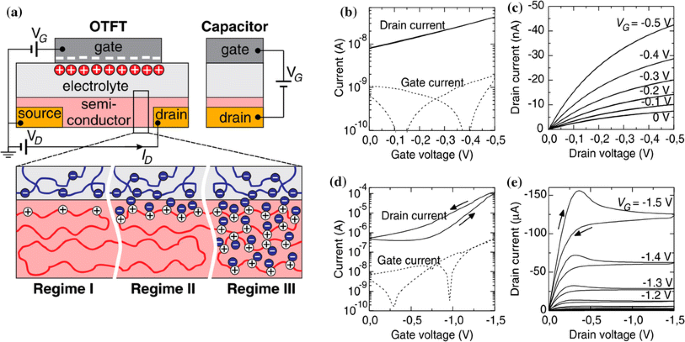
Electric double-layer transistors: a review of recent progress
![Electrical Double Layer based devices](https://www.researchgate.net/publication/346595241/figure/fig1/AS:1002301418401794@1615978688749/Illustration-of-the-electrical-double-layer-model-d-is-the-thickness-of.png)
Illustration of the electrical double-layer model; δ is the thickness
![Electrical Double Layer based devices](http://www.archie-west.ac.uk/wp-content/uploads/2013/10/Picture1.jpg)
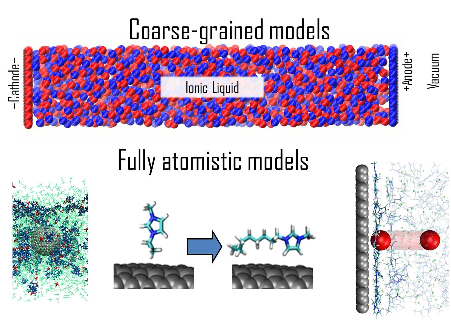
Interfacial Properties of Room-Temperature Ionic Liquids: Electrical Double Layer, RTILs&Nanomaterials and Applications – ARCHIE-WeSt
from
per adult (price varies by group size)