Balancing Layers in Your PCB Layout
By A Mystery Man Writer
Description
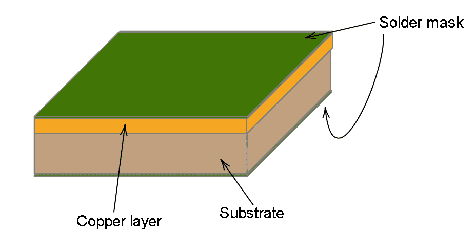
Balancing layers in your PCB layout stack-up, which both layer surfaces and cross-sectional structure of the circuit board are reasonably symmetrical.
![Balancing Layers in Your PCB Layout](https://circuitdigest.com/sites/default/files/field/image/Layer-Stacking-in-PCB-Design.jpg)
An Overview of Layer Stack Management in PCB Design
![Balancing Layers in Your PCB Layout](https://www.altium.com/documentation/sites/default/files/wiki_attachments/320797/LSM_Rigid-FlexSelection_Advanced.png)
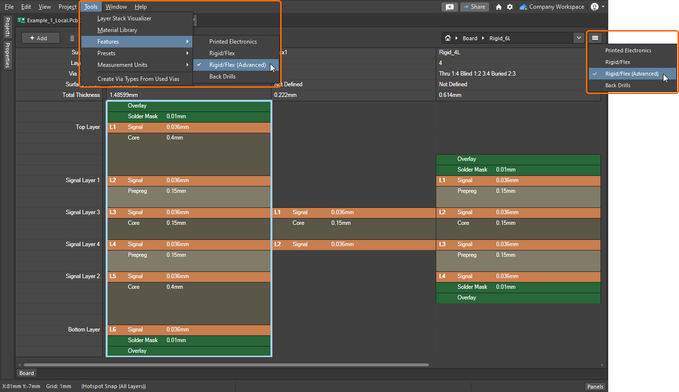
Defining the Layer Stack in Altium Designer Altium Designer 24 Technical Documentation
![Balancing Layers in Your PCB Layout](https://media.springernature.com/m685/springer-static/image/art%3A10.1038%2Fs41586-022-04992-8/MediaObjects/41586_2022_4992_Fig1_HTML.png)
A compute-in-memory chip based on resistive random-access memory
![Balancing Layers in Your PCB Layout](https://blog.epectec.com/hubfs/pcb-with-wraparound-edge-plating.jpg)
Epec's Blog Printed Circuit Boards (7)
![Balancing Layers in Your PCB Layout](https://resources.altium.com/sites/default/files/blogs/How%20to%20Create%20a%20PCB%20Layout%20from%20a%20Schematic%20in%20Altium%20Designer-67862.jpg)
How to Create a PCB Layout from a Schematic in Altium Designer
![Balancing Layers in Your PCB Layout](https://img.youtube.com/vi/9Uaz4vthw_8/hqdefault.jpg)
Design Guidelines for IPC Class 3 PCBs
![Balancing Layers in Your PCB Layout](https://www.circuitbasics.com/wp-content/uploads/2021/07/singleLayerPCB.png)
Best Practices for Designing a PCB Layout - Circuit Basics
![Balancing Layers in Your PCB Layout](https://www.multi-circuit-boards.eu/fileadmin/img/03_Design-Hilfe/kupfer-balance/pcb_copper_balance_symmetrical_layer-buildup.gif)
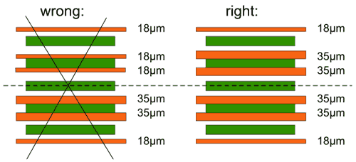
Copper balance - Multi Circuit Boards
![Balancing Layers in Your PCB Layout](https://www.pcbcart.com/Uploads/Editor/2017-12-12/5a2fa9c60a7ea.jpg)
PCB Layer Stackup, PCB Stackup Design
![Balancing Layers in Your PCB Layout](https://resources.altium.com/sites/default/files/blogs/PCB%20Trace%20and%20Pad%20Clearance%3A%20Low%20vs.%20High%20Voltage-76478.jpg)
PCB Trace and Pad Clearance: Low vs. High Voltage, PCB Design Blog
![Balancing Layers in Your PCB Layout](https://www.mktpcb.com/wp-content/uploads/2021/06/Types-of-PCB-Layers.jpg)
PCB Layers: Everything You Need to Know
![Balancing Layers in Your PCB Layout](https://blog.epectec.com/hubfs/pcb-layer-with-segregated-differential-pairs.jpg)
Epec's Blog Printed Circuit Boards (7)
from
per adult (price varies by group size)